我们课题组主要利用分子束外延和激光分子束外延方法构筑精细的界面结构并研究界面处演生的新奇量子现象。近期我们主要关注的材料体系包括过渡金属氧化物、二维材料以及它们构成的异质结。我们常用的表征手段包括:STEM, EELS, 原子分辨的EELS图,PPMS, SHG, SQUID 和低温 MFM.
We focus on the construction of delicate crystal structures via molecular beam epitaxy (MBE) and Laser MBE and studying the emergent phenomena at interfaces of related materials. Recently, we are focusing on transition metal oxides (eg. LCMO, SrRuO3, LSCO), two dimensional materials (eg. Bi2O2Se, FeSe) and their heterostructures. Our characterization methods contain STEM, EELS, atomically resolved EELS mapping, PPMS, SHG, SQUID and LT MFM.
界面量子态
Interface quantum states

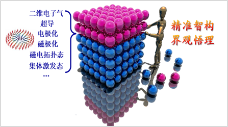
由于对称性破缺导致对电荷、轨道、自旋和晶格之间的复杂耦合作用的影响,关联材料异质界面演生出许多与相应体材所不同的丰富物理性质。通过构筑精准的界面结构,获得界面二维电子气及奇异磁电量子态。
By the perturbation of broken symmetry on the subtle close coupling between charge, orbital, spin and lattice degrees of freedom, Hetero-interfaces of correlated electron materials exhibits a lot of emergent properties which are fundamentally different from their bulk counterparts。 Through constructing delicate heterostructures, Here we focus on explore some fascinating phenomena, such as two dimensional electron gas and anomalous quantum electro-magnetic states.
铜基界面超导
Cuprate interface superconductivity

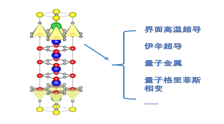
揭示铜基高温超导的微观机理被《科学》选为125个重要科学问题之一,同时也是凝聚态物理的最大的未解之谜之一。利用OMBE原子尺度下的外延生长,我们着力研究铜基界面超导研究,以此提供研究反常高温超导和新型量子态的平台。
Revealing the microscopic nature of high-temperature superconductivity in cuprates has been selected as one of the 125 major scientific problems in Science, which is still one of the biggest mysteries and challenges in condensed matter physics. By exploiting OMBE growth in atomic precision, we study the interface superconductivity in cuprate materials which also provide important platforms for exploring unconventional high-Tc superconductivity and new quantum states in general.
高迁移率二维半导体
High mobility 2D
semiconductor

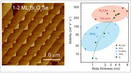
高迁移率二维半导体材料是构筑 “后硅时代” 电子器件和集成电路的理想沟道材料。Bi2O2是近年来发现的一种高迁移率二维半导体材料,其优点显著,主要包括:空气稳定性高、带隙合适、载流子有效质量低、电子迁移率高、制备简单等。我们主要利用分子束外延方法制备超薄Bi2O2薄膜,并基于此构筑铁磁性高迁移率二维半导体。
High mobility two-dimensional materials are ideal channel materials for post-silicon electronics and integrated circuits. Bi2O2, a two-dimensional semiconductor material with high mobility, was discovered in 2017. The advantages of 2D Bi2O2 mainly include air stability, suitable band gap, low effective carrier mass, high electron mobility and simple preparation. We focus on the molecular beam epitaxy of ultra-thin Bi2O2 film and construction of ferromagnetic high-mobility 2D semiconductor.
界面态探测方法研究
Probing technique study for
interface states

当前缺少合适的高空间、高能/动量分辨率的表征手段,来定量观测界面磁电量子态。本课题组拟发展多尺度多方式联合的磁电结构表征平台,勾勒出界面磁电结构及相应集体行为。
There is currently a lack of suitable high-spatial, high-energy/momentum resolution technique to quantitatively observe the interfacial states. We intend to develop a multi-scale and multiple probing platform to microscopically reveal interface electronic and magnetic structure as well as related collective behavior.
 中国科学院物理研究所 Institute of Physics Chinese Academy of Sciences